DalisAndy
Hazard to Others

Posts: 129
Registered: 8-5-2015
Member Is Offline
Mood: No Mood
|
|
PCB etchant
I'm considering doing a project that requires me to make custom PCBs. I have been reading up on different ways to etch a copper board. I was curious
if any of you guys have tried PCB echting? What would be the most easily to redo and would be the safest? I was going to show my FRC robotics team
how to make PCBs. That way I would like it to be the safest option and the easiest to repeat
Elements Collected: 19/81 (Excluding all radioactive, using placecard for those)
Any tips or good sources are welcome.
|
|
|
aga
Forum Drunkard
Posts: 7030
Registered: 25-3-2014
Member Is Offline
|
|
Photoresist PCB off ebay.
Get Laser-ok transparent film
Print your PCB onto that with a laser printer
UV lightbox
Expose the board for 2 mins
Devlop in the developer recommended for that photoresist
Etch in ferric chloride (iron wool in HCl for a while).
Did two today.
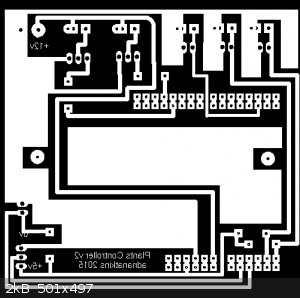
This a simple carrier board for an Ardunino uno to water plants and monitor some things.
Ew ! the image looks nasty. The board looks better.
Edit:
The big ground planes are not for any RF or Heat considerations : it just etches quicker if there is less copper to etch away.
[Edited on 18-10-2015 by aga]
|
|
|
m1tanker78
National Hazard
Posts: 685
Registered: 5-1-2011
Member Is Offline
Mood: No Mood
|
|
Use your favorite PCB layout program to generate a mirror image of your PCB (preferably in vector format).
Use the 'dark' setting on a laser printer to print the 1:1 scaled image onto your favorite photographic paper.
Iron the image onto a very clean PCB - image side down.
Soak the PCB/adhered paper in warm soapy water for some time.
Peel whatever paper you can off the PCB. You may need to use gentle scrubbing in some areas and/or soak for longer period of time.
Once all paper residue is removed and only the toner remains, immerse the board in a shallow plastic container with HCl (muriatic acid). Add about
equal volume of 3% drugstore hydrogen peroxide and agitate the solution gently until all copper has dissolved from non-toner areas of board. Should
take from between 1 and 5 minutes depending on temperature and such.
Rinse PCB thoroughly and remove the toner with acetone, toluene or fine stainless scouring pad.
***************************
Keep fingerprints and oils off the PCB throughout process.
Don't leave PCB in etching solution longer than needed - traces will undercut.
Be diligent when you iron the image onto PCB. Use the high end of the heat setting. It's almost impossible to burn the paper/PCB with a normal
household clothes iron.
Wear gloves and etch the board outdoors. Avoid breathing HCl fumes.
I've used this method for 15+ years and have great results even with very fine pitch traces/component pads. Not too difficult for the beginner. No
fancy resist/developer chems or lamps needed. Board can be etched in under 5 minutes.
Chemical CURIOSITY KILLED THE CATalyst.
|
|
|
DalisAndy
Hazard to Others
Posts: 129
Registered: 8-5-2015
Member Is Offline
Mood: No Mood
|
|
On the steel wool one. Fe +2 can't be oxidized to +3 by HCl. You would have to add an oxidizer to it.
Elements Collected: 19/81 (Excluding all radioactive, using placecard for those)
Any tips or good sources are welcome.
|
|
|
WGTR
National Hazard
Posts: 971
Registered: 29-9-2013
Location: Online
Member Is Offline
Mood: Outline
|
|
This topic is something that I have a lot of personal experience with! I also did a demonstration for a local robotics team, where I showed them how
to make circuit boards. There was a lot of excitement in the room that day.
I generally agree with aga, however, there are certain things I'd suggest that would make this easier, less expensive, and more
repeatable. The exact method for how this is best done depends on variables such as:
1. Is this the start of a long-term hobby, or are you just making one PCB, and then never doing it again?
2. Do you plan on making just a few pieces of many different PCB designs, or perhaps many copies of few designs?
3. How much cost can you absorb up front?
4. Do you want to do primarily single-layer boards, two-layer, or multilayer? Do you need the holes plated through, or are bus wire vias sufficient?
5. Do you plan to drill your boards by hand, or do you have access to a CNC mill for this task? Or alternately, will you not use holes at all?
Buying a copper-clad board that is pre-coated with resist is OK, but I generally don't like doing this. My reasoning is that it gets expensive over
time. If you mess up (and you probably will when starting out), then you have to buy another pre-coated board before you can try again. I personally
prefer laminating the board with resist myself, that way I can experiment with the photographic process to my heart's content without having to waste
the expensive copper-clad board. The resist by itself is generally pretty inexpensive.
I like to use a dry film resist sold by Think & Tinker. I've used this product for about 15 years, and my processes are developed around it. It's about $125 for a 100' roll, but it
will last you a very long time unless you are doing production work. Keep it in a dark, air-conditioned, dry place, like a closet,
and it will keep for 5-10 years (much longer than they say).
They say to handle the film in a darkroom, but that's not completely necessary. Fluorescent light has a slow, but cumulative effect on the film. For
this reason, I cut pieces from the roll in a darkened room. The cut pieces however, can be safely handled in normal fluorescent lighting as long as
the exposure time isn't excessive (say, 10-15 minutes). Incandescent lighting is preferable, if available, due to its lack of UV output. It's
generally safe to handle the roll in dim incandescent lighting.
The film comes protected with a cover film, and a backing film. The cover film stays on until the film is ready for developing. The backing needs to
be removed before laminating the film onto the copper. To do this, put two pieces of Scotch tape together on one edge of the film, and pull them
apart. 9 times out of 10, the backing film comes off with the tape, leaving the cover film in place.
Degrease the copper surface, scrub it with an abrasive cleaner, and clean it again. Wear gloves, and don't touch the copper with bare fingers,
otherwise you'll have adhesion problems. After the board is clean and dry, place it down flat on some paper towels, and cover the copper surface with
a 1-2% ethanol solution. Backing side down, the film is floated onto the copper surface, and the excess solvent is gently worked out from under the
film. Don't leave any bubbles. The film needs to be bonded tightly to the copper, and it takes pressure to do this. For small (<2"x2") boards
I'll fold up a paper towel, and then use it to add increasing pressure to the film as I rub from the center out towards the edges. If you add to much
pressure too soon, the film will wrinkle. For larger boards, I have a hard rubber roller (about 1.5" dia.) that I absconded from an old typewriter.
Leaning into the board with everything I have, I roll it across the film very slowly. Whichever method is used, the film is sufficiently close to the
copper when you can see the weave of the fibreglass (under the copper) on the surface of the film.
From there, the board is placed into an oven at 200F for 10 minutes. This fully bonds the film to the copper. If there are air bubbles present under
the film afterwards, you didn't add enough pressure when laminating the film, and too much solvent was left.
After the laminated board cools down (face-side down, to keep it from room light), it is ready for exposure. The negative artwork is placed
emulsion side down onto the copper, and it is held close to the surface by means of a weighted piece of glass. This glass needs to be cheap, clear,
window glass (like from Home Depot). The green-colored art glass from hobby stores usually blocks UV, and is pretty useless. My exposure source is a
500W quartz-halogen work lamp ($10-20 at Home Depot!). The bulb is about 12" away from the film, and the exposure time is generally 1-2 minutes. The
exposure time varies depending upon the age of the photo-resist (measured in years), and will have to be played with a bit.
The exposed film is developed with a warm 2-5% sodium carbonate (washing soda) solution. At this point I like to keep the film in relative darkness,
but soft incandescent lighting poses no problems. After the board has been swished around in developer for about 30 seconds, the cover sheet should
come right off under water. Don't tug vigorously on the cover sheet, it should come off easily when it's ready. The board is swished around in the
developer, and the photo-resist is rubbed gently with the finger tips. The board should appear to be fully developed after about 5 minutes. It is
lying to you. After twice that amount of time (10 minutes) the board should be fully developed.
Artwork is one of those things that can be done several different ways. It depends on what your application is. Laser printing negatives onto
transparency film does work, but the artwork needs to be doubled or tripled up, and each layer needs to be perfectly registered to obtain good
resolution. Even though the ink appears dark, it doesn't block UV sufficiently when just one layer is used. It usually works OK for one-offs.
Personally, I like to use a film output service. Screen printers use this type of service extensively, because they need film to make their
screens. Basically, you send them an image file of your layout, and they mail you the negatives within a day or two. In my own city, there are
several companies that do this, and it is trivial to go retrieve the film the following morning. One company that does this posts their prices here. I haven't done business with them before, though. This type of film is designed specifically for your application, and can be used over
and over again for multiple boards. You will be much happier with proper film negatives than laser printed transparencies, because the high contrast
of the film gives you much more leeway on photo-resist exposure times. In other words, it's harder to overexpose photo-resist when using
high-contrast film.
Once the board is fully developed, it can be lightly brushed with a soft brush, just to make sure that there isn't any residual film clinging to the
bare copper areas. Rinse and dry, and then heat in an oven again at 200F for 10 minutes before etching.
Ferric chloride is the way to go for class demonstrations. It's quick, relatively safe, and not overly aggressive. HCl/CuCl2 etchant
would give less undercutting, but it takes too long for classroom work. The missing oxidizer in your ferrous chloride is hydrogen peroxide. 3% is OK
to use for this, but it will water down the etchant. It will be necessary to concentrate the etchant afterwards by evaporating it down on a hot
plate. Heat the solution until all of the excess hydrogen peroxide decomposes. You don't want this present when you finally etch
your boards. If brown sludge develops during concentration, add small amounts of HCl until it all dissolves. I really don't think
HCl/H2O2 etchant is a good idea. It's far too aggressive, and it gasses.
After the board is etched, the etch resist can be removed easily by soaking in acetone. Now, show off your brand new PCB to wowed onlookers...
[Edited on 10-19-2015 by WGTR]
|
|
|
Twospoons
International Hazard
Posts: 1282
Registered: 26-7-2004
Location: Middle Earth
Member Is Offline
Mood: A trace of hope...
|
|
I have used the toner transfer method successfully for many years, as outlined above by m1tanker78. My only additional comments are to use 'toner
transfer paper' designed for the process, as it gives a better result and easier separation of paper from the tone. better still is paper called
Press'n'Peel Blue (actually its mylar film with a coating), as the release layer also seals the toner surface and reduces pin-holing. Primary causes
of failure are dust or grease on the copper before transfer.
Best etchant: ferric chloride. I've tried HCl/peroxide and also ammonium persulfate. FeCl3 may be messy, but its given me the best results.
Best ever result: double-sided Kapton flex pcb with 0.005" track/space. Only 1 circuit in a panel of 24 failed!
Helicopter: "helico" -> spiral, "pter" -> with wings
|
|
|
m1tanker78
National Hazard
Posts: 685
Registered: 5-1-2011
Member Is Offline
Mood: No Mood
|
|
Quote: Originally posted by Twospoons  | better still is paper called Press'n'Peel Blue (actually its mylar film with a coating), as the release layer also seals the toner surface and reduces
pin-holing.
Best etchant: ferric chloride. I've tried HCl/peroxide and also ammonium persulfate. FeCl3 may be messy, but its given me the best results.
|
Good call. I've used Press'n'Peel in the past and had excellent results. In a pinch, regular photographic paper (glossy) works just fine if you don't
mind putting a little elbow grease and patience into the removal. I usually just soak the board and paper in water for ~1 hour and then go to work on
it. It comes off very easily with help from a toothbrush. Nowadays I exclusively use a cheap 'house' brand of photo paper from office depot.
As to the aggressiveness of HCl/H2O2: aggressiveness is the name of the game. Back in college, we used to leave our boards overnight in a ferric
chloride bath on top of a stepper motor-driven tilting platform (for agitation). The professor would put the boards in a rinse bin for us first thing
in the morning. There was also the uncertainty of the freshness of the resist and the exposure time. Blughhh..
I should add that the aggressiveness can be controlled by how much hydrogen peroxide is added. Just in case anyone is wondering about disposal, the
spent solution finds excellent use in swimming pools to raise copper level in place of [usually] copper sulfate. The copper can be precipitated as the
hydroxide/carbonate salt by simply neutralizing the spent solution with lye or sodium bicarbonate. The solution can be reused 2 or 3 times but it's
better to start fresh and use small quantities (hence the shallow container).
Fun times!
Chemical CURIOSITY KILLED THE CATalyst.
|
|
|
NeutralIon
Harmless
Posts: 28
Registered: 19-6-2005
Member Is Offline
Mood: No Mood
|
|
I have successfully made printed circuit boards at home -- here are some of my notes for doing so:
Board:
Use pre-sensitized board with positive resist -- don't try applying the resist to a regular board, it is very difficult to do it right without proper
equipment. Suitable boards are made by Injectorall (available at DigiKey) and GC (available at Jameco). [If anyone has had success applying resist
please post your method for doing so.]
Artwork:
Best to create the artwork on a computer. I use the gschem and pcb programs that are part of the free gnu Electronic Design Application (gEDA) suite.
There are other programs that can also be used. Take your time and be sure the artwork is what you want in the final board. When using a positive
resist board black lines on the artwork will give copper traces on the finished board.
Print the artwork on a transparency. I get best results with hp premium inkjet transparency film. Make sure you print on the "rough' side. Set
printer to print black only and for "best" printing.
Safe Light:
The board must be handled under a red safe light until it is developed. I made a safelight using 12 red LEDs [LITEON LTL2P3SEK (available from
DigiKey)] in 3 series strings of 4 diodes each and with a 0.25W, 200Ω resistor in series with each string. Applying 12 V gives about 14 mA thru each
diode and a total light output of about 40000 mcd. Red Christmas tree lights would probably work.
Exposure:
Place the printed side of the transparency in contact with the sensitized copper and clamp these between 2 pieces of glass -- do under safe light.
Expose the boards to a UV light, such as from a pair of FT15T8-BL bulbs. These bulbs are available from DigiKey; they may also be available locally
at an electrical supply store. DO NOT use BLB bulbs, the so called "black light" bulbs sold in party stores -- these have a coating that block the UV
spectrum needed to expose the board.
Best to make some small boards and experiment with the time and distance needed to get the right exposure with your setup. For my setup using a pair
of FT15T8-BL bulbs and with the board in its glass sandwich located about 4.5 inches from the centerline of the bulbs, the following exposure times
gave good results [YMMV]:
Injectorall: 30 to 35 minutes.
GC: 10 minutes.
Developing:
I develop my boards in a solution of sodium metasilicate (Na2SiO3) -- Red Devil TSP/90, available at hardware stores as a heavy duty cleaner, is
Na2SiO3.5H2O. I generally make a 0.6M stock solution of Na2SiO3 by dissolving 64 grams of TSP/90 in approximately 400 ml of heated water and then add
distilled water to make a final volume of 500 mL. I then dilute that to make the proper working developer for the board I am using:
Injectorall: 0.3M [1 part developer stock to 1 part water].
GC: 0.24M [2 parts developer stock to 3 parts water].
Some sources suggest using NaOH as a developer -- I don't recommend that. It is very hard to get the right balance of developer strength, temperature
and time and is therefore prone to complete over developing or not developing at all.
Develop under a safe light. Use a large enough container to allow the board to be moved around and use sufficient developer to cover the board.
Rough rule of thumb: approximately 6 mL of Na2SiO3 developer for each square cm of board [double that for a 2 sided board]. Developing time tends to
be:
100 to 120 seconds for Injectorall boards.
60 to 80 seconds for GC boards.
If the pattern appears to be completely developed rinse the board for about 30 seconds in cold water. At this point regular lights may be turned on
and a more thorough examination made of the board. If all looks well rinse again for about 2 minutes in a fresh batch of cold water, followed by a
final rinse by squirting distilled water on the board as it is held vertically. Failure to properly rinse may result in some traces going missing.
One way to test if the board is fully developed is to dunk it in the etchant for about 10 seconds then examine the board to see if all the areas that
are to be cleared of copper are a reddish color and not the normal copper color -- this shows that the etchant is attacking the copper. If there are
un-developed areas rinse the board and put it back in the developer.
Etching:
There are several different chemicals that will etch copper but I prefer Cupric Chloride and HCl. There are 2 reasons for that: 1)You can make it at
home with scrap copper and some hardware store HCl -- No need to have it shipped to you with Hazmat fees; and 2)It can be regenerated over and over
and over...
The etching reaction is:
CuCl2 + Cu + HCl -> 2CuCl + HCl
[The HCl is just there to provide an acidic environment to allow the reaction to proceed.]
The regeneration reaction is:
2CuCl + 2HCl + ½O2 -> 2CuCl2 + H2O
[You get back twice as much CuCl2 as you used in the etching.]
To make the initial batch (500 mL) of CuCl2 etchant:
Put 60 gm of scrap Cu (stranded line cord with many fine copper strands is ideal) and 50 mL of HCl in a glass jar. The jar should be at least 50%
larger than the intended batch size. Cover and shake the jar so that the HCl wets the copper wire. Let stand 3 days with the cover loosened --
preferably outside. The solution should be an opaque brown and the exposed copper should have a blue-green crust on it. Then add 300 mL HCl and 150
mL H2O to the jar. Cover the jar with a cap with a 0.25" hole drilled in it. Connect an aquarium air pump to some tubing and put the other end of
the tubing thru the hole and into the solution. Turn on the air pump and run it until all the copper is disolved and the solution is a transparent
emerald green -- could take 1 to 2 weeks depending on temperature and air flow. [Yes, this is a rather long time but you can use this first batch to
etch some small test boards to determine the optimum exposure time, and meanwhile make a second batch of etchant.]
Final Notes:
After developing the board will still have resist covering the copper traces -- this can be easily removed with acetone. I generally leave the resist
on until after I drill the board and am ready to solder the components.
Credit where credit is due: The procedure for making the etchant is from the web site: http://members.optusnet.com.au/eseychell/PCB/etching_CuCl/in...
That link seems to be dead now but copies are available onother sites.
Using the procedures described above I have been able to make good printed circuit boards with traces as small as 10 mils and spacings as small as 5
mils.
Knowledge is Good
|
|
|
nlegaux
Hazard to Self
Posts: 93
Registered: 28-11-2014
Location: East Tennessee
Member Is Offline
Mood: No Mood
|
|
In the past I have gotten some okay results using sharpie as a mask (just in case you want to go the cheap way!).
nlegaux
|
|
|
Twospoons
International Hazard
Posts: 1282
Registered: 26-7-2004
Location: Middle Earth
Member Is Offline
Mood: A trace of hope...
|
|
There is another method, if you have access to a CO2 laser engraver. You can spray the bare copper with a thin layer of paint, then laser off the
parts you want etched away. The relatively low power (>100W) CO2 lasers wont touch the copper, but can happily evaporate paint.
Helicopter: "helico" -> spiral, "pter" -> with wings
|
|
|
bquirky
Hazard to Others
Posts: 316
Registered: 22-10-2008
Location: Perth Western Australia
Member Is Offline
Mood: No Mood
|
|
| Quote: Originally posted by Twospoons | | There is another method, if you have access to a CO2 laser engraver. You can spray the bare copper with a thin layer of paint, then laser off the
parts you want etched away. The relatively low power (>100W) CO2 lasers wont touch the copper, but can happily evaporate paint.
|
I do alot of pcb's this way and have found that I get the best results if i let the copper significantly oxidize first and then spray a thin coat of
polyurethane ontop. i prepare a whole batch of 'blank's this way and just squirt some acetone on them after etching to get the polyurethane off.
I found my 40W laser would leave a very thin layer of polyurethane near the clean shiny copper un-molested regardless of exposure time. i think this
may be a mechanical cooling effect of the copper or some kind of near field / standing wave effect of the very very long wavelength co2 laser
reflecting off the copper.
|
|
|
Twospoons
International Hazard
Posts: 1282
Registered: 26-7-2004
Location: Middle Earth
Member Is Offline
Mood: A trace of hope...
|
|
Its definitely a mechanical cooling effect. Metal cutting lasers need fairly high power densities because of the heat dissipation of the metal
surrounding the cut.
With your 40W laser, using a shorter focusing optic would allow you to reduce your spot size and increase power density (up to a point - its limited
by beam quality and wavelength) - allowing better paint ablation performance.
There's also a paint I've used for metal marking, where the laser sets the paint hard, and un-lasered paint washes off in water. Works as an etch
resist, but the paint is rather expensive.
[Edited on 27-10-2015 by Twospoons]
Helicopter: "helico" -> spiral, "pter" -> with wings
|
|
|
|