experimental
Harmless

Posts: 21
Registered: 9-7-2017
Member Is Offline
Mood: curious
|
|
new way of PCB via plating
In this thread I'm reporting the success of a new way of plating vias in PCBs.
For those not into electronics, the goal is to chemically deposit copper into holes of a printed circuit board to make them conductive. The hole walls
are made of fiberglass, which is non conductive. Electrolytic plating is thus not possible until a way is found to deposit a first conductive layer on
the hole walls.
Many ways have been proposed, including a solution using calcium hypophosphite, which is a controlled substance, and a solution using expensive
palladium chloride activator and formaldehyde. This link details the known methods in greater detail
http://www.instructables.com/id/Inexpensive-method-of-indust...
Quite a while ago NurdRage has shown how to make a silver conductive ink using far less exotic chemicals, and I wondered if it could be used to
deposit the first conductive layer on the PCB holes.
Today I finally tried, and it worked.
After drilling a few holes, immersing the board in a sodium hydroxide solution for cleaning, applying the conductive ink to the holes and heating the
board for a few minutes, the hole sides were covered in grey silver, which looked promising.
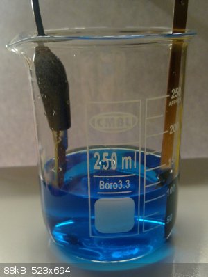
The next step was to try electroplating copper and see if the silver coating works. For this I used the formula shown in a comment to the
instructables link:
100mL water
20g CuSO4*5H2O
6g H2SO4
0.1g Polyethylene glycol
1 drop of copper chloride solution
and immersed the PCB and a copper electrode. I plated for 50 minutes at 0.5A, around 250mA/cm^2.
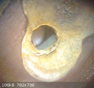
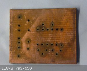
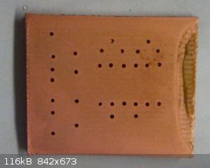
The holes were covered in copper, and the resistance is quite low, less than 0.1 ohm.
Bottom side
Top side with plated copper (note that I used a single sided PCB just to more easily test the conductivity of each hole)
|
|
|
Twospoons
International Hazard
Posts: 1280
Registered: 26-7-2004
Location: Middle Earth
Member Is Offline
Mood: A trace of hope...
|
|
Did you weigh the pcb before and after to determine how much copper was plated out?
Helicopter: "helico" -> spiral, "pter" -> with wings
|
|
|
aga
Forum Drunkard
Posts: 7030
Registered: 25-3-2014
Member Is Offline
|
|
Nice work !
It will probably be easier with a double-sided PCB.
|
|
|
experimental
Harmless
Posts: 21
Registered: 9-7-2017
Member Is Offline
Mood: curious
|
|
I have not weighed the pcb unfortunately, but I'll be doing more experiments in the next days.
|
|
|
experimental
Harmless
Posts: 21
Registered: 9-7-2017
Member Is Offline
Mood: curious
|
|
During the past month I made many experiments for making double sided printed circuits at home, but I always failed at making a working PCB, despite
being annoyingly so close to getting it right.
As I don't (yet?) have a youtube channel, I'm writing what I learned in this post hoping it may be useful to someone else.
All experiments start with a piece of double sided copper clad PCB, which is first drilled to make the holes that will be later made conductive. Fine
sandpaper is used to smooth the hole edges, the board is then washed to remove debris, and immersed in a solution of NaOH to clean any dirt and
fingerprints that were observed to affect the following steps. The board is put on a hotplate until it is perfectly dry.
Then a drop NurdRage's conductive silver ink is applied inside each hole using a micropipette. It is important to not smear the ink around the holes,
as it silver plates the copper preventing etching and thus shorting traces of the PCB. It turns out this is both tedious and difficult. The board is
put on a hotplate to dry the ink, and then washed with water.
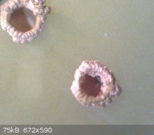
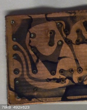
Despite the bad picture, the board is covered in the original copper it came with, and conductive silver has been deposited inside the holes. Now it's
time to electrolytically deposit more copper, using the copper plating solution that I described in a previous post.
This step is the one that works best in the entire process, although after some uses the plating starts becoming nonuniform. To fix this, it is enough
to add a bit more PEG. The solution must also be decanted from time to time to remove the copper dust that is formed by the copper electrode. After
this step all holes are copper plated.
Very fine sandpaper is used to smooth the copper surface, silver ink is reapplied to all holes and dried in an attempt to protect the copper inside
the holes from etching away at a later step, and then the photoresist is applied.
It turns out that applying spray photoresist uniformly to both sides of the board is very difficult. The photoresist does not apply evenly, and after
being exposed and developed leaves marks that short traces together. Also, using the silver ink for protecting the holes does not work very well.
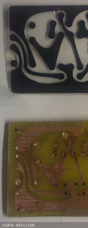
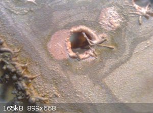
After etching in a solution of copper chloride and HCl, the board looks like this. Compared to the mask used for exposing it has shorts between
traces, and part of the copper inside some holes has been etched away.
It turns out better solutions are needed for basically each step. A copper ink would be much better for making the holes conductive, a simple way to
coat the board in photoresist is needed, maybe spin coating, but how to do coat both sides? as well as a way to protect the holes, perhaps
electrolytic silver plating?
|
|
|
RogueRose
International Hazard
Posts: 1585
Registered: 16-6-2014
Member Is Offline
|
|
This is great work and i've researched a way to make PCB's as well. I'm confused as to why the holed need plated, doesn't the entire piece of
fiberglass need to be plated, or if it already is plated, then the copper already there is adequate for the wire to be connected?
|
|
|
Twospoons
International Hazard
Posts: 1280
Registered: 26-7-2004
Location: Middle Earth
Member Is Offline
Mood: A trace of hope...
|
|
Quote: Originally posted by RogueRose  | | I'm confused as to why the holed need plated, doesn't the entire piece of fiberglass need to be plated, or if it already is plated, then the copper
already there is adequate for the wire to be connected? |
1]Without plating in the holes it is necessary to solder top and bottom. With some components it is very difficult to solder on the component side
(radial electrolytics being the first that comes to mind) as the part is designed to fit flush against the PCB and the top pad is concealed.
2] plated holes are also used to make vias - a connection from one side to the other that does not have a component lead in it. Vias are frequently
used under other parts, making joining with a scrap of wire difficult or impossible.
Now it is possible to design around these limitations, but that can really limit your design options, hence the desire for homebrew plated holes. Also
soldering twice is a PITA.
The commercial process uses a palladium activator for the hole walls ( which must be de-smeared of epoxy to expose the glass fiber), followed by an
electroless copper plate to make the walls conductive, followed by electrolytic copper to build thickness. This also builds the trackwork to the
desired thickness After that the pcb pattern is plated on in tin, using a negative of the artwork. The tin also plates down the holes. The the
artwork is stripped,and the exposed copper etched away - the tin acting as a resist. Next the tin is stripped, leaving a bare copper pattern. Finally
a solder mask is screen printed on, and the desired surface finish applied to the exposed pads (HASL, ENIG, silver, organic mask).
[Edited on 21-1-2018 by Twospoons]
Helicopter: "helico" -> spiral, "pter" -> with wings
|
|
|
RogueRose
International Hazard
Posts: 1585
Registered: 16-6-2014
Member Is Offline
|
|
| Quote: Originally posted by Twospoons | | Quote: Originally posted by RogueRose | | I'm confused as to why the holed need plated, doesn't the entire piece of fiberglass need to be plated, or if it already is plated, then the copper
already there is adequate for the wire to be connected? |
1]Without plating in the holes it is necessary to solder top and bottom. With some components it is very difficult to solder on the component side
(radial electrolytics being the first that comes to mind) as the part is designed to fit flush against the PCB and the top pad is concealed.
2] plated holes are also used to make vias - a connection from one side to the other that does not have a component lead in it. Vias are frequently
used under other parts, making joining with a scrap of wire difficult or impossible.
Now it is possible to design around these limitations, but that can really limit your design options, hence the desire for homebrew plated holes. Also
soldering twice is a PITA.
The commercial process uses a palladium activator for the hole walls ( which must be de-smeared of epoxy to expose the glass fiber), followed by an
electroless copper plate to make the walls conductive, followed by electrolytic copper to build thickness. This also builds the trackwork to the
desired thickness After that the pcb pattern is plated on in tin, using a negative of the artwork. The tin also plates down the holes. The the
artwork is stripped,and the exposed copper etched away - the tin acting as a resist. Next the tin is stripped, leaving a bare copper pattern. Finally
a solder mask is screen printed on, and the desired surface finish applied to the exposed pads (HASL, ENIG, silver, organic mask).
[Edited on 21-1-2018 by Twospoons] |
Thanks for the explination! That makes a lot of sense about the vias as well as component mounting. I had never seen these on a lot of the how-to
guides where people make their own PCB's - it was simple trace the leads and etch then drill holes, but that is almost always for single sided PCB's.
If there is anything that others could help you with, I'd be happy to try some things out as I've been looking for a way to make PCB's (coating them
with copper) for a while now. It'd be interesting if there was a way to re-use old PCB's in some way as IDK if it is easy to find blank fibergalss
PCB's and I hate paying $5-8 for a 4"x6" copper plated PCB..
I have plenty of CuSO4 and FeCl2 or other things to etch boards.
|
|
|
experimental
Harmless
Posts: 21
Registered: 9-7-2017
Member Is Offline
Mood: curious
|
|
Since NurdRage's silver ink is made with silver acetate, ammonia and formic acid, I tried to use copper acetate instead, hoping to make an ink that
would deposit copper. Honestly I had very little confidence that it would work, and as expected, it didn't work.
|
|
|
zed
International Hazard
Posts: 2277
Registered: 6-9-2008
Location: Great State of Jefferson, City of Portland
Member Is Offline
Mood: Semi-repentant Sith Lord
|
|
Yup! Most experiments fail.
|
|
|
aga
Forum Drunkard
Posts: 7030
Registered: 25-3-2014
Member Is Offline
|
|
Experiments only fail or succeed when someone actually Does an experiment.
Good work experimental.
Keep trying.
|
|
|
Bezaleel
Hazard to Others
Posts: 444
Registered: 28-2-2009
Member Is Offline
Mood: transitional
|
|
I appreciate your effort, experimental. The majority of my experiments also fail when trying out something new.
|
|
|