| Pages:
1
2 |
wish i had a kraken!!!
Hazard to Others

Posts: 157
Registered: 22-3-2012
Member Is Offline
Mood: No Mood
|
|
A very simple circuit created on a piece of glass

|
|
|
DrMario
Hazard to Others
Posts: 332
Registered: 22-9-2014
Member Is Offline
Mood: Underpaid.
|
|
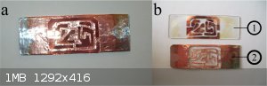
Is that a PCB glued to a microscope slide?
I recognize the circuit, BTW: it's an astable multivibrator with two bipolar transistors.
[Edited on 29-10-2014 by DrMario]
|
|
|
wish i had a kraken!!!
Hazard to Others
Posts: 157
Registered: 22-3-2012
Member Is Offline
Mood: No Mood
|
|
Dear DrMario , U have trained eyes! yes , It is an astable multivibrator with two bipolar transistors ! :-) BUT U know it is coated on Microscope
Slider!
[Edited on 29-10-2014 by wish i had a kraken!!!]
Masked Slider right after being coated by copper!
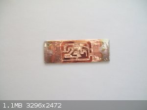
[Edited on 29-10-2014 by wish i had a kraken!!!]
[Edited on 29-10-2014 by wish i had a kraken!!!]
|
|
|
WGTR
National Hazard
Posts: 971
Registered: 29-9-2013
Location: Online
Member Is Offline
Mood: Outline
|
|
Good Job!
Did you use adhesive-backed copper tape, or did you glue copper foil to the glass with epoxy, and then etch? How did you etch it, mechanically or
chemically?
|
|
|
Praxichys
International Hazard
Posts: 1063
Registered: 31-7-2013
Location: Detroit, Michigan, USA
Member Is Offline
Mood: Coprecipitated
|
|
I'm secretly hoping the answer is sputtering followed by electron beam lithography.
|
|
|
WGTR
National Hazard
Posts: 971
Registered: 29-9-2013
Location: Online
Member Is Offline
Mood: Outline
|
|
I'm afraid it looks like foil, attached with some type of adhesive!
I did the same thing once, with copper foil and epoxy. The foil was pressed onto the glass with an old typewriter roller. The idea was to push out
almost all of the epoxy from under the copper. From there, the foil was masked with photo-film and exposed to UV through a positive. After
developing, and then etching with ferric chloride, the circuit board pattern on glass was used as a negative for other exposures.
At the time, I was interested in making durable negatives for production PCB work, but I have moved on to other methods.
|
|
|
wish i had a kraken!!!
Hazard to Others
Posts: 157
Registered: 22-3-2012
Member Is Offline
Mood: No Mood
|
|
Quote: Originally posted by WGTR  | | Did you use adhesive-backed copper tape, or did you glue copper foil to the glass with epoxy, and then etch? How did you etch it, mechanically or
chemically? |
I did not used adhesive-backed copper tape :-D I used sputtering instead , First I draw the circuit lines on a pice of Al foil then using a sharp
razor I cut the lines out after that I covered the Microscope slider with the foil the I sputtered it !
|
|
|
wish i had a kraken!!!
Hazard to Others
Posts: 157
Registered: 22-3-2012
Member Is Offline
Mood: No Mood
|
|
Bravo :-) U nailed it ! It is sputtering but I did not used electron beam lithography (I don't have such a thing yet !)
|
|
|
DrMario
Hazard to Others
Posts: 332
Registered: 22-9-2014
Member Is Offline
Mood: Underpaid.
|
|
I'm partly with you: I hope it's sputtering of an adhesive layer (titanium, chromium or Ti/W) and then copper on top.
However, to achieve a thick enough layer for soldering, copper should be electrodeposited. With sputtering you can deposit up to about 2 µm of copper
before the lab technician releases the hound dogs at you (at 1 µm they already start barking). Not enough for soldering.
BUT THEN... no electron beam because that's too freaking slow. Even one mm2 of surface patterned by electron beam lithography can take from a quarter
of an hour to an hour.
No - my hope is that the poster used the best tool for the job: traditional lithography.
But the quality of the surface tells me that this probably is not the case.
|
|
|
DrMario
Hazard to Others
Posts: 332
Registered: 22-9-2014
Member Is Offline
Mood: Underpaid.
|
|
| Quote: Originally posted by wish i had a kraken!!! | | Quote: Originally posted by WGTR | | Did you use adhesive-backed copper tape, or did you glue copper foil to the glass with epoxy, and then etch? How did you etch it, mechanically or
chemically? |
I did not used adhesive-backed copper tape :-D I used sputtering instead , First I draw the circuit lines on a pice of Al foil then using a sharp
razor I cut the lines out after that I covered the Microscope slider with the foil the I sputtered it !
|
So you used the aluminium foil as shadow mask?
EDIT: more questions: did you use an adhesion layer? How thick is your copper layer? Finally: isn't this a rather expensive way to make such a simple
circuit board? There's also the fact that this is less robust than normal PCBs, for several reasons. It is more thermally resistant than a PCB, but
the elements themselves aren't, anyway.
I can, however, appreciate the exercise. However, at our institution, every hour of sputter time costs 100 EUR. Unless you have sputtered that
microscope slide alongside your main sample, you've saddled a project with a non-negligible expenditure.
[Edited on 29-10-2014 by DrMario]
|
|
|
jock88
National Hazard
Posts: 505
Registered: 13-12-2012
Member Is Offline
Mood: No Mood
|
|
Why is sputtering so expensive?
Can a dude not make his own sputtering apparatus.
You do need a vacuum system buts after that it all plain sailing???????
|
|
|
DrMario
Hazard to Others
Posts: 332
Registered: 22-9-2014
Member Is Offline
Mood: Underpaid.
|
|
Unless it's one of those mini sputters used to deposit a few nm of gold on samples for SEM, it's an expensive piece of kit (high fixed cost) and it
usually needs maintenance by an engineer with considerable experience with vacuum technology. This person's salary is a running cost. In our case,
some of our vacuum equipment (one sputter, one RIE, one PECVD, a DRIE and yes, one of those cheap little sputters outside of the cleanroom) is
maintained by an actual researcher. Yes, there's some cost in maintaining the external pump that runs 24/7, there's some cost in the form of target
consumption, etc. And of course, since this is a research cleanroom the targets need to be replaced/rotated from time to time - usually tungsten is
swapped for platinum, and chromium and titanium may be swapped sometimes.
All this adds up.
Now we do have one of those cheapo mini sputters outside of the cleanroom, but that thing is not suitable for depositing significant amounts of
material, it can only have one target at a time, and still needs maintenance. So it's cheaper than the big sputters, but we still get to pay
€50/hour for usage.
|
|
|
Dr.Bob
International Hazard
Posts: 2662
Registered: 26-1-2011
Location: USA - NC
Member Is Offline
Mood: No Mood
|
|
Wow, I worked with some E-beam lithography about 30 years ago, and yes, it was slower than watching paint dry, but able to make some incredibly
complex chips very well and with what were very fine lines back then. Did a coop doing mostly photolithography using photoresists on silicon wafers.
It was a neat experience, but then I went into more organic chemistry, since most of the chemistry of electronics was really nasty back then. We
used boiling sulfuric acid, HF, PH3, AsH3, and many other lovely compounds. Also NF3 and others to clean CVD chambers. I mostly did the cross
linking work, testing various condinions, which was boring compared to much of the other work. But I helped fix other things as well. That was so
long ago that the chips were not even CMOS, but old NPN type. Wish I had kept more of the stuff from them, it would be great for the Smithsonian. I
do still have some Core memory somewhere...
[Edited on 30-10-2014 by Dr.Bob]
|
|
|
DrMario
Hazard to Others
Posts: 332
Registered: 22-9-2014
Member Is Offline
Mood: Underpaid.
|
|
I'll hazard a guess that you used phosphine and arsine (lovely name, that) only for ion implantation. Our ion implanter uses phosphine, arsine and
borine. The main user of the ion implanter suggested running as fast as possible, should there be any leak of these gases, but generally I feel rather
safe, as these aren't handled in a manual way and there is a lot of fool-proof mechanisms built into that godawful, huge and loud machine.
The etchant solution haven't gotten any nicer since you worked in a cleanroom, though EDP or hydrazine are thankfully not used for crystallographic
etching of silicon, anymore. On the other hand, TMAH crystallographic etching is very popular, in spite of the fact that it can release some
battlefield gases with some silicon dopants.
Chlorine gas is used for DRIE, along with the much more docile SF6 (I guess DRIE wasn't yet used, back when you were doing your bipolar transistor
ICs).
HF is as common as ever. We use tons of the stuff.
So all in all, I'd say things have not become much safer, although our safety protocols are annoyingly thorough. I've yet to work in any chemistry lab
that has even close to the safety margins that we employ, but I won't bore you with details.
|
|
|
wish i had a kraken!!!
Hazard to Others
Posts: 157
Registered: 22-3-2012
Member Is Offline
Mood: No Mood
|
|
| Quote: Originally posted by DrMario |
I'm partly with you: I hope it's sputtering of an adhesive layer (titanium, chromium or Ti/W) and then copper on top.
However, to achieve a thick enough layer for soldering, copper should be electrodeposited. With sputtering you can deposit up to about 2 µm of copper
before the lab technician releases the hound dogs at you (at 1 µm they already start barking). Not enough for soldering.
BUT THEN... no electron beam because that's too freaking slow. Even one mm2 of surface patterned by electron beam lithography can take from a quarter
of an hour to an hour.
No - my hope is that the poster used the best tool for the job: traditional lithography.
But the quality of the surface tells me that this probably is not the case. |
Dear DrMario I did not used adhesive layers such as those U mentioned I just used Copper , and :-) I didn't feel worry about hound dogs! Cuz I used
(and am using) my own made sputter coater :-)
DrMario I don't know anything about the thickness of coated
layer (I used my homemade sputter coater it is not equiped with the device which monitors the thickness of coated layer )
If U know any practical method for measuring the thickness of coated layer I would be really glad if U share it with me :-).
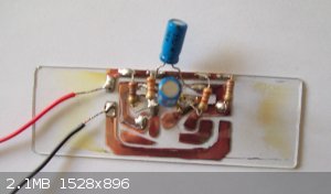
I did not want to use this method for making PCBs I just wanted to show that my homemade sputter coater is capable of depositing a layer of copper , I
then mounted electronic components to prove that I have achived a good sputter coated layer of Copper. :-)
[Edited on 30-10-2014 by wish i had a kraken!!!]
|
|
|
DrMario
Hazard to Others
Posts: 332
Registered: 22-9-2014
Member Is Offline
Mood: Underpaid.
|
|
| Quote: Originally posted by wish i had a kraken!!! |
Dear DrMario I did not used adhesive layers such as those U mentioned I just used Copper , and :-) I didn't feel worry about hound dogs! Cuz I used
(and am using) my own made sputter coater :-)
|
I am very impressed!!! Can you please share more info on your self-made sputter? Some pics? Diagrams? Maybe make a youtube video of it?
Do you also make your own targets, or do you buy commercial ones? What other targets, in addition to copper, do you have?
Do you have a turbopump?
Is it a DC or an AC sputter?
|
|
|
wish i had a kraken!!!
Hazard to Others
Posts: 157
Registered: 22-3-2012
Member Is Offline
Mood: No Mood
|
|
| Quote: Originally posted by DrMario | | Quote: Originally posted by wish i had a kraken!!! |
Dear DrMario I did not used adhesive layers such as those U mentioned I just used Copper , and :-) I didn't feel worry about hound dogs! Cuz I used
(and am using) my own made sputter coater :-)
|
I am very impressed!!! Can you please share more info on your self-made sputter? Some pics? Diagrams? Maybe make a youtube video of it?
Do you also make your own targets, or do you buy commercial ones? What other targets, in addition to copper, do you have?
Do you have a turbopump?
Is it a DC or an AC sputter? |
Happy to hear that :-) It is a DC-magnetron sputter coater , I don't have a turbopump :-( (Just a vacum pump capabale of reaching 0.02 mbar ), And I
tested Aluminium and it was not a successful test then I am going to test Ti soon :-)
|
|
|
wish i had a kraken!!!
Hazard to Others
Posts: 157
Registered: 22-3-2012
Member Is Offline
Mood: No Mood
|
|
U can see Plasma and sample holder :-)
In my design cathode is located at the buttom but soon I became aware that this is not a good design and needs to be changed ;-)
[Edited on 30-10-2014 by wish i had a kraken!!!]

|
|
|
WGTR
National Hazard
Posts: 971
Registered: 29-9-2013
Location: Online
Member Is Offline
Mood: Outline
|
|
Woop! Woop!
"Fun police, here! There have been reports of someone having too much fun in the lab. We are here to investigate. Yup, looks like we're going to
have to write you a ticket."
This is quite an interesting project. I didn't realize at first what you did, since the aluminum foil looked like copper. I use a small sputter
coater for SEM work, but don't use it for other things since it takes so long to pump down. For copper plating glass I either use electroless copper
onto silver or electroplated copper onto conductive glass. How much money do you have invested in the project? How long did it take you to put the
project together? Did you follow a set of plans, or develop it yourself?
Pretty cool.
|
|
|
wish i had a kraken!!!
Hazard to Others
Posts: 157
Registered: 22-3-2012
Member Is Offline
Mood: No Mood
|
|
| Quote: Originally posted by WGTR | Woop! Woop!
"Fun police, here! There have been reports of someone having too much fun in the lab. We are here to investigate. Yup, looks like we're going to
have to write you a ticket."
This is quite an interesting project. I didn't realize at first what you did, since the aluminum foil looked like copper. I use a small sputter
coater for SEM work, but don't use it for other things since it takes so long to pump down. For copper plating glass I either use electroless copper
onto silver or electroplated copper onto conductive glass. How much money do you have invested in the project? How long did it take you to put the
project together? Did you follow a set of plans, or develop it yourself?
Pretty cool.
|
HAHAHAHA , Hope they(Fun Police) won't send me to the jail!
I will give U more info about it or maybe I will add a topic in technochemistry
for now watch these pics :-)
[Edited on 31-10-2014 by wish i had a kraken!!!]
|
|
|
DrMario
Hazard to Others
Posts: 332
Registered: 22-9-2014
Member Is Offline
Mood: Underpaid.
|
|
| Quote: Originally posted by wish i had a kraken!!! | U can see Plasma and sample holder :-)
In my design cathode is located at the buttom but soon I became aware that this is not a good design and needs to be changed ;-)
[Edited on 30-10-2014 by wish i had a kraken!!!] |
Please give us/me more info, diagrams, instructions, pump model.... or else I will call the fun police! Or something!!
BTW, if you had trouble sputtering Al, you'll have even more trouble sputtering Ti. If you can get ahold of tungsten, try that. Also nickel.
|
|
|
wish i had a kraken!!!
Hazard to Others
Posts: 157
Registered: 22-3-2012
Member Is Offline
Mood: No Mood
|
|
| Quote: Originally posted by DrMario | | Quote: Originally posted by wish i had a kraken!!! | U can see Plasma and sample holder :-)
In my design cathode is located at the buttom but soon I became aware that this is not a good design and needs to be changed ;-)
[Edited on 30-10-2014 by wish i had a kraken!!!] |
Please give us/me more info, diagrams, instructions, pump model.... or else I will call the fun police! Or something!!
BTW, if you had trouble sputtering Al, you'll have even more trouble sputtering Ti. If you can get ahold of tungsten, try that. Also nickel.
|
Dear DrMario , soon I will give U more info about it in fact I have plans to add a topic about it in technochemistry :-D
I don't know what is wrong with Aluminium , maybe it requires lower vaccum pressur , maybe insted of Ar I should use Ne , I really don't Know! :-(
I really don't know what to do with Al !!! I really applogize my Language but it is a real pain in the ass!
[Edited on 31-10-2014 by wish i had a kraken!!!]
[Edited on 31-10-2014 by wish i had a kraken!!!]
|
|
|
DrMario
Hazard to Others
Posts: 332
Registered: 22-9-2014
Member Is Offline
Mood: Underpaid.
|
|
| Quote: Originally posted by wish i had a kraken!!! |
I don't know what is wrong with Aluminium , maybe it requires lower vaccum pressur , maybe insted of Ar I should use Ne , I really don't Know! :-(
I really don't know what to do with Al !!! I really applogize my Language but it is a real pain in the ass!
|
I think it's pretty simple: aluminium is very reactive and will create oxide and nitride even in low pressure air. Basically what you're doing is
reactive sputtering (i.e. sputtering in a reactive atmosphere).
In any case, I don't think you should replace Argon with Neon. Neon's ionization energy is 21.5 eV, quite a bit higher than Argon's.
|
|
|
wish i had a kraken!!!
Hazard to Others
Posts: 157
Registered: 22-3-2012
Member Is Offline
Mood: No Mood
|
|
| Quote: Originally posted by DrMario | | Quote: Originally posted by wish i had a kraken!!! |
I don't know what is wrong with Aluminium , maybe it requires lower vaccum pressur , maybe insted of Ar I should use Ne , I really don't Know! :-(
I really don't know what to do with Al !!! I really applogize my Language but it is a real pain in the ass!
|
I think it's pretty simple: aluminium is very reactive and will create oxide and nitride even in low pressure air. Basically what you're doing is
reactive sputtering (i.e. sputtering in a reactive atmosphere).
In any case, I don't think you should replace Argon with Neon. Neon's ionization energy is 21.5 eV, quite a bit higher than Argon's.
|
I filled the chamber with Ar and then vaccumed it and .... so I think there is no chance for Al to be Oxidized !
I also think it is not a good Idea to replace Ar But I wanted to replace Ar by Ne because Ne ions are lighter than Ar ions and I think Ar Ions have
too much energy which cause in inefficiency of sputtering of Al ! but I am not Sure!
[Edited on 31-10-2014 by wish i had a kraken!!!]
|
|
|
wish i had a kraken!!!
Hazard to Others
Posts: 157
Registered: 22-3-2012
Member Is Offline
Mood: No Mood
|
|
I just made a video of it ! U can see it here : https://www.youtube.com/watch?v=VGmFLUNf0nE
|
|
|
| Pages:
1
2 |